Nov 20, 2023
X-Rays Are Becoming an Essential Health Check-Up in Chipmaking
, Bloomberg News

(Bloomberg) -- Omron Corp., a Japanese provider of health-care equipment and factory automation, is setting its sights on the lucrative chipmaking gear market to fuel future growth.
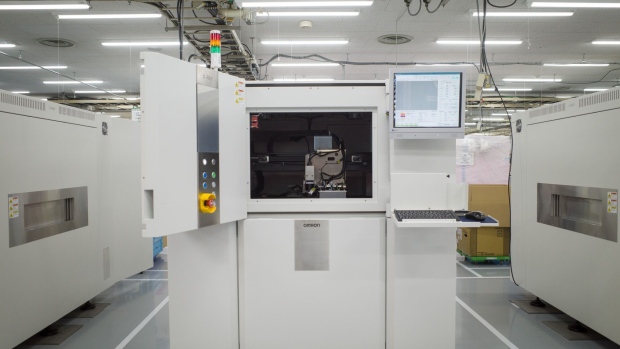
The Kyoto-based electronics firm is launching an X-ray scanner in the spring that will better detect flaws in advanced semiconductor manufacturing and improve production yields for the world’s biggest chipmakers. The VT-X950 machine will produce 3D images of chips with sufficient resolution to identify defects at a 1-nanometer scale, at least a generation ahead of the current best-in-class silicon fabrication techniques.
Because the scans only take 30 seconds each, a chipmaker can monitor production at close to real time and make adjustments and corrections more efficiently. The yield, or proportion of defect-free chips produced from each silicon wafer, is a closely watched metric for fabricators like Taiwan Semiconductor Manufacturing Co. and Samsung Electronics Co. — it affects each firm’s costs and speed in fulfilling customer orders.
“The demand trend in the semiconductor industry is to make a wider variety of chips in smaller lots, but that would never be economically feasible without real-time CT scanning,” Omron’s general manager of inspection systems Kazuhisa Shibuya said in an interview.
CT, or computed tomography, is a mainstay of medical diagnostics and has also become an essential quality control tool in chipmaking. Ninety-year-old Omron, which earns more than half of its ¥876 billion ($5.9 billion) annual revenue from factory automation products, first entered the semiconductor supply chain in 2012 with the release of its VT-X900. That remains a small part of its business, largely limited to a few major chipmakers, Shibuya said.
The 55-year-old official is confident that demand will grow as chips become ever more complex and expensive to manufacture. In an area of just a few square centimeters, makers need to write metal lines that are thinner than a human hair and deposit thousands of nanoscale solder bumps. New techniques of stacking chips into three-dimensional structures — such as TSMC and Samsung’s gate-all-around architectures — raise the precision requirements.
“The need for CT scans as part of the semiconductor manufacturing process is urgent,” Omdia analyst Akira Minamikawa said. “As the industry pursues die shrinking and chiplet technology, the level of bonding technology required has soared, especially in the last couple of years.”
Today’s most in-demand chips, Nvidia Corp.’s top-of-the-line artificial intelligence accelerators, are bottlenecked by TSMC’s ability to produce the advanced packaging to encase them. Quality control and yield improvement become paramount in such circumstances, as a tiny misalignment can make chips that sell for tens of thousands of dollars worthless. X-raying chips as they are made can help detect imperfections and allow workers to fine-tune the process as needed.
Sony Group Corp.’s share price dropped 4.7% earlier this month after the company said it’s having trouble mass-producing its newest smartphone camera sensor, which ended up pushing down the business’ operating profit outlook by 15%.
Traditionally, chipmakers have relied on so-called function tests to see whether a device will operate as designed. CT has also been used, but at a much slower pace: picking up sample units from production lines to conduct X-ray checks at a separate room that can take up to an hour each. The need for faster inspection machines will increase drastically, according to Toyo Securities analyst Hideki Yasuda. The cost of cutting-edge chip manufacturing will dictate more real-time monitoring to minimize wasted silicon, he said.
Omron’s CT scanners are the only realistic option for chipmakers to install on their assembly lines, Shibuya said, as no other machines can produce high-quality CT images in real time. The latest model slashes the time of a scan by half from Omron’s previous model.
©2023 Bloomberg L.P.


